


The PATGEN4 peripheral lets you output arbitrary 4 bit patterns of up to a length of 4096 patterns. The frequency of the output and the length (1-4096) of the pattern is programmable.
Hardware:
The PATGEN4 peripheral uses a 4x4K block of RAM in the FPGA to store a user defined pattern. An address counter is initialized to zero and the four bit pattern at address zero is placed on the output pins. The address counter is incremented at a user defined rate. As the address counter is incremented the pattern at that address is placed on the output pins. Incrementing the address counter continues until the address reaches a user defined terminal count. The address counter is set back to zero on the count after the terminal count.
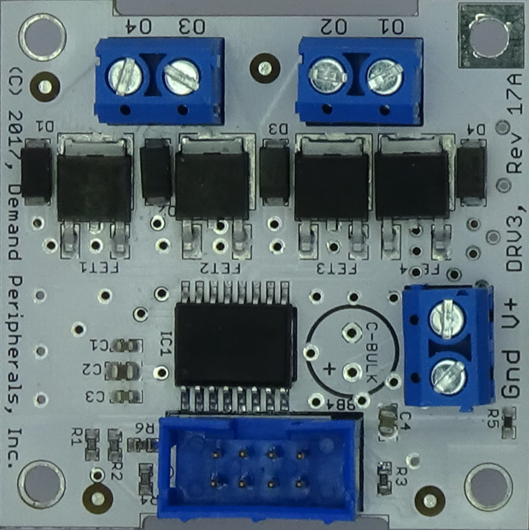
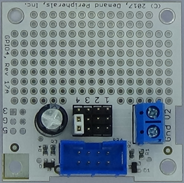
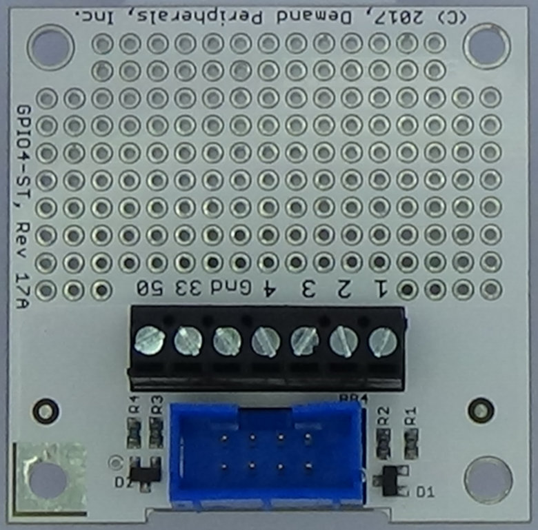
The lowest numbered pin on the connector is controlled by the LSB in the four bit patterns. PATGEN4 works with any of the following cards: GPIO with pin headers GPIO with screw terminals Open-Drain Driver Card
Resources:
pattern : the address and pattern data. This resource lets you incrementally fill the pattern RAM with data. The address is given first as a 12 bit hex value. The values starting at that address are given as a string of hex characters. You can specify up to 64 hex values with each pcset command. This resource is write-only and only works with pcset. For example, the following commands fill the first 128 four-bit nibbles with an alternating pattern of 0101 and 1010.
    pcset patgen4 pattern 000 5a5a5a5a5a5a5a5a5a5a5a5a5a5a5a5a5a5a5a5a5a5a5a5a5a5a5a5a5a5a5a5a
    pcset patgen4 pattern 040 5a5a5a5a5a5a5a5a5a5a5a5a5a5a5a5a5a5a5a5a5a5a5a5a5a5a5a5a5a5a5a5a
config : clock rate and maximum address.
The config resource has the clock rate in Hertz followed
by the maximum pattern address as a 12 bit hex value.
The actual clock rate might not be exactly the value you
specify. A pcget on the config resource returns the
actual clock rate.
Examples:
Consider a hypothetical problem in which you want to send an SPI packet to a device, wait a short time, and send it again. You are ignoring the return values. MOSI is on the LSB, an active low chip enable is on the next LSB, and SCK is on the MSB. The SPI packet to send is c455, the SCK frequency should be 500 KHz, and the SPI port is Mode 0 with MSB first. The pattern clock will be at 1 MHz since it has to be twice the SCK frequency. The hex string, c455, is 1100010001010101 in binary. For each binary bit we set the data bit and the clock low, then set the clock high. Chip select goes low before the first bit and high after the last bit. Putting this all together as a set of commands to the PATGEN4 peripheral you'd get:
    pcset patgen4 pattern 000 0191908080819080808190819081908190
    pcset patgen4 pattern 022 222222222222222222222222222222
    pcset patgen config 1000000 03f